Microscopy
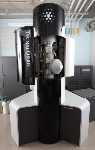
CanmetMATERIALS hosts state-of-the-art electron microscopes that provide world-class characterization and micro-analytical capabilities, including high-end field-emission scanning electron microscopes (SEM), a dual-beam focused ion beam (FIB) microscope and a field-emission transmission electron microscope (TEM), along with a complete suite of metallography facilities including optical microscopes, micro-indentation and a digital image analyser.
The high-resolution SEM has a thin window energy-dispersive X-ray detector (EDS) for qualitative chemical composition analysis, a wavelength X-ray spectrometer for quantitative composition analysis, and an electron backscattered diffraction pattern detector (EBSD) for phase identifications and micro-texture studies.
The dual-beam FIB is also equipped with EDS and EBSD and is capable of imaging and analysing cross-sections within specimens and enabling serial sectioning, circuit editing and preparation of TEM-ready samples.
The TEM is equipped with state-of-the-art analytical systems such as the ChemiSTEM™ technology, which provides fast EDS analysis and elemental mapping, and an electron energy loss spectrometer (EELS), which is capable of performing chemical analysis of lighter elements.
Page details
- Date modified:
